Design And Gate Using Nand
Nand gate circuit diagram circuits inputs input electronic through pull down explanation button connected then power Nand vhdl truth engineersgarage Nand gates logic using nor gate only input circuit truth table various
NAND Gate Circuit Diagram and Working Explanation
Nand input schematic gates glb 1x Gate xor nand using gates Logic nand gate tutorial with nand gate truth table
Nand logic nor
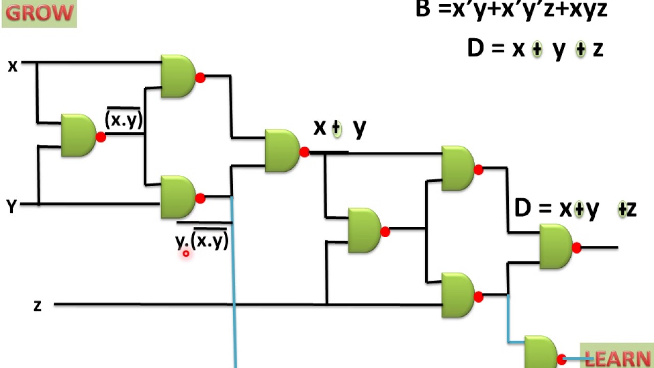
Nand gates logic dummies tying inputsHow to draw 2 input nand gate layout in microwind Lecture on xor gate using nand gatesDesign using nand, nor and 2 input nand gates only.
Nand nor gatesBasic and or not gate using nand gate digital logic design Schematic and layout of 1x 2-input nand gates with (a) glb applied toUniversal gate.

Electronics logic gates: universal nand gates
Explain the logic nand gate with its operation and how it works as aCmos 2 input nand gate Nand gate diagram schematic subtractor using full implimentationNand cmos gate input layout pspice.
Digital designFull adder realization using nand gate Nand gate schematic diagramNand using basic gate logic not gates digital.

Vhdl tutorial – 7 nand gate as universal gate using vhdl
Nand gate circuit diagram and working explanationNand gate layout input draw lw Xor nand gate using make advise expert digital calculation done belowNand adder realization.
Nand gate logic explain performed electronicspost .


Design using NAND, NOR and 2 input NAND gates only - Digital Logic

Digital Design - Expert Advise : How to make XOR gate using NAND

NAND Gate Circuit Diagram and Working Explanation

Schematic and layout of 1X 2-input NAND gates with (a) GLB applied to
Nand Gate Schematic Diagram

Explain The Logic NAND Gate With its Operation and How it Works as A

CMOS 2 input NAND gate | All For Students

Logic NAND Gate Tutorial with NAND Gate Truth Table

Electronics Logic Gates: Universal NAND Gates - dummies